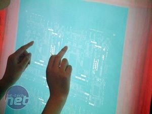
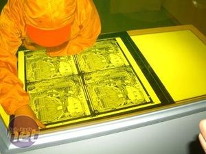
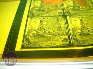
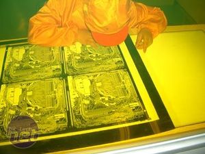
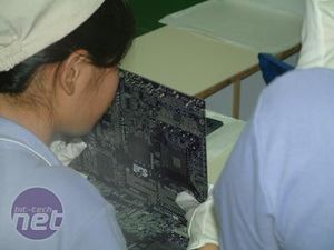
The prints created by the Alignment Exposure Unit are closely examined by a number of workers, in order to check that all traces are healthy and complete. Once this process is completed, the circuits are etched into the PCB.
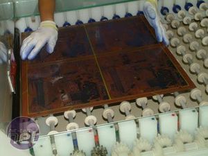
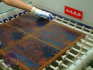
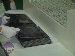
Once the etching process is complete, the D/F lamination layer is removed and the PCB is rinsed. The PCB then moves onto the solder mask stage. This is where the PCB begins to resemble something you'd find in your home computer. The PCB is dyed - this is basically a surface treatment to protect and cover up the traces underneath it. Obviously, this requires quite a bit of curing time before the PCB can move to the next stage.
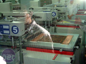
After the solder mask stage has been completed, the board is given its surface treatment. During this stage, all holes on the PCB are treated at the same time with Nickel Gold Plating. Also, logos, branding, model numbers and information about the boards' features are printed on the PCB.



Want to comment? Please log in.