First Look: Nvidia nForce 790i Ultra SLI
March 19, 2008 | 08:16

From what we understand, the price difference between both nForce 790i versions is quite significant, but the feature difference is marginal: the “Ultra” moniker products are only better tuned to support faster memory and offer more aggressive overclocking (although both are designed to provide significant overclocking headroom).
The standard SLI version is limited to EPP 2.0 at 1,333MHz whereas the nForce 790i Ultra SLI will support DDR3 EPP 2.0 up to 2,000MHz. Both chipset versions are DDR3 only – Nvidia has chosen to optimise the chipset for one memory type specifically so this should yield better performance on its own.
From previous experience, DDR3 only really comes into its own over 1,600MHz, so we find it difficult to understand why anyone willing to pay for such a performance product will not do it the justice of buying performance parts to complement it. Considering the price of DDR2, the performance overlap between “standard” DDR3 at 1,333MHz and an nForce 780i SLI with (EPP) DDR2 at ~1,200MHz should be negligible considering the large price difference.
However, both nForce 790i products also include native 1,600MHz FSB CPU support, where the nForce 780i SLI didn’t (but could still overclock easily enough to offer unofficial support). This is understandable as only Intel’s niche performance parts will feature the fastest FSB, so those looking to buy such expensive CPUs will likely want to pair them with technology such as multi-multi-GPU and DDR3 available here.

EPP 2.0 for DDR3 works in exactly the same way as EPP 1.0 does with DDR2, but it includes extra data specific to DDR3 that is needed to guarantee the increase in performance and reliability. By buying memory with EPP 2.0 support included, you’re effectively buying a guaranteed overclock because the modules have been tested and qualified to work at the sold frequency. Enabling the EPP function in the BIOS will automatically set the elevated frequency and voltages that were qualified.
Obviously you can do things manually and try for more if you like – it’s not a fixed function in the same way EPP 1.0 and Intel’s XMP are. A point worth noting is that XMP modules are not compatible with EPP 2.0 and vice versa – even though Nvidia is keen to reiterate that that EPP 2.0 is an open standard, like ESA, it’s very rare that competitors will use each other’s technology because it’s not of mutual benefit.
The other advantage of DDR3 over DDR2 is that now the memory-FSB ratios can be set in sync at 1:1. On the DDR2 boards, general performance and overclocking was increased by this setting as the north bridge latencies were greatly reduced when both bus speeds are synchronised. This should provide the key to the expected performance increases for the nForce 790i series, as reduced chipset latencies are also touted as the key to the Intel X48 series.
What will be interesting to see is if Nvidia allows the same kind of core chipset timing manipulation like Asus has achieved with the Intel X48 on its upcoming Rampage – will you get to play with the key tRD timing (among others) in the BIOS on the Striker II Extreme? There is the general "Sync" setting and even new "P1/P2" options that control the "internal timing parameters" but nothing really specific to know what value it's starting from, at least with the reference design.
Nvidia was keen to point out that the reference BIOS has been designed to make overclocking as easy as possible – by leaving most of the voltages default it will increase them automatically according to elevated bus frequencies: very clever. We hope this technology permeates down to the mainstream boards in time, where people with less knowledge can achieve better value through easier overclocking. If anything, hardcore enthusiasts who are buying this will very likely want to do everything manually.
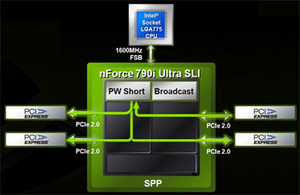
What you won’t see on nForce 790i series boards is the NF200 chipset present on the nForce 780i and 750i SLI boards – this has now been integrated into the north bridge. It includes the same two technologies: the Posted-Write Shortcut (PWShort) that allows the GPUs in SLI to remain in sync with fewer commands, cutting out the need to visit main memory, and GPU Broadcast, which the CPU only has to send the data once to address multiple GPUs.
This technology is predominantly optimised for standard SLI, as just two PCI-Express 2.0 x16 lanes are spurned from the north bridge – the third slot that is used for 3-way SLI comes from the south bridge and that doesn’t feature the new SLI technologies. This might add extra latency and stress to the HyperTransport link, but the larger 3-way SLI bridge connector handles most of the GPU-GPU inter communication.
The standard SLI version is limited to EPP 2.0 at 1,333MHz whereas the nForce 790i Ultra SLI will support DDR3 EPP 2.0 up to 2,000MHz. Both chipset versions are DDR3 only – Nvidia has chosen to optimise the chipset for one memory type specifically so this should yield better performance on its own.
From previous experience, DDR3 only really comes into its own over 1,600MHz, so we find it difficult to understand why anyone willing to pay for such a performance product will not do it the justice of buying performance parts to complement it. Considering the price of DDR2, the performance overlap between “standard” DDR3 at 1,333MHz and an nForce 780i SLI with (EPP) DDR2 at ~1,200MHz should be negligible considering the large price difference.
However, both nForce 790i products also include native 1,600MHz FSB CPU support, where the nForce 780i SLI didn’t (but could still overclock easily enough to offer unofficial support). This is understandable as only Intel’s niche performance parts will feature the fastest FSB, so those looking to buy such expensive CPUs will likely want to pair them with technology such as multi-multi-GPU and DDR3 available here.

EPP 2.0 for DDR3 works in exactly the same way as EPP 1.0 does with DDR2, but it includes extra data specific to DDR3 that is needed to guarantee the increase in performance and reliability. By buying memory with EPP 2.0 support included, you’re effectively buying a guaranteed overclock because the modules have been tested and qualified to work at the sold frequency. Enabling the EPP function in the BIOS will automatically set the elevated frequency and voltages that were qualified.
Obviously you can do things manually and try for more if you like – it’s not a fixed function in the same way EPP 1.0 and Intel’s XMP are. A point worth noting is that XMP modules are not compatible with EPP 2.0 and vice versa – even though Nvidia is keen to reiterate that that EPP 2.0 is an open standard, like ESA, it’s very rare that competitors will use each other’s technology because it’s not of mutual benefit.
The other advantage of DDR3 over DDR2 is that now the memory-FSB ratios can be set in sync at 1:1. On the DDR2 boards, general performance and overclocking was increased by this setting as the north bridge latencies were greatly reduced when both bus speeds are synchronised. This should provide the key to the expected performance increases for the nForce 790i series, as reduced chipset latencies are also touted as the key to the Intel X48 series.
What will be interesting to see is if Nvidia allows the same kind of core chipset timing manipulation like Asus has achieved with the Intel X48 on its upcoming Rampage – will you get to play with the key tRD timing (among others) in the BIOS on the Striker II Extreme? There is the general "Sync" setting and even new "P1/P2" options that control the "internal timing parameters" but nothing really specific to know what value it's starting from, at least with the reference design.
Nvidia was keen to point out that the reference BIOS has been designed to make overclocking as easy as possible – by leaving most of the voltages default it will increase them automatically according to elevated bus frequencies: very clever. We hope this technology permeates down to the mainstream boards in time, where people with less knowledge can achieve better value through easier overclocking. If anything, hardcore enthusiasts who are buying this will very likely want to do everything manually.
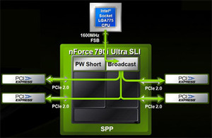
What you won’t see on nForce 790i series boards is the NF200 chipset present on the nForce 780i and 750i SLI boards – this has now been integrated into the north bridge. It includes the same two technologies: the Posted-Write Shortcut (PWShort) that allows the GPUs in SLI to remain in sync with fewer commands, cutting out the need to visit main memory, and GPU Broadcast, which the CPU only has to send the data once to address multiple GPUs.
This technology is predominantly optimised for standard SLI, as just two PCI-Express 2.0 x16 lanes are spurned from the north bridge – the third slot that is used for 3-way SLI comes from the south bridge and that doesn’t feature the new SLI technologies. This might add extra latency and stress to the HyperTransport link, but the larger 3-way SLI bridge connector handles most of the GPU-GPU inter communication.

MSI MPG Velox 100R Chassis Review
October 14 2021 | 15:04


Want to comment? Please log in.