AMD's New Brazos Blatform: E-350 APU and Hudson M1 FCH
Manufacturer: AMDWith all the yapping about Intel's Sandy Bridge over the last few months, it's great to actually write something about AMD for a change. We remember discussing the future of Fusion with AMD in 2007, and back then it all seemed very promising. This just goes to show the difference made by a few years. This was before the economic kerfuffle, before Clarkdale and before AMD spun-off its fabrication wing to form GlobalFoundries. Four years later, it seems unbelievable that we finally have a Fusion CPU in our mitts to test.
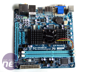
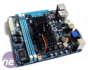
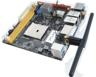
We've already covered several mini-ITX Fusion boards in our early preview. However, Gigabyte was the first company to get us a retail sample, ahead of the official release at the end of February.
We'll get back to the Gigabyte board on the next page, but first let's get into the details of AMD's new APU.
APU? In case you haven't been following the latest tech news closely, APU is AMD's new term to describe the evolution of its CPU. The increasing complexity of CPUs has been a constant trend of progression: the integration of the FPU (maths co-processor) in the early 90s, the integration of the memory controller in the AMD64 architecture in 2003. Then we had the PCI-E controller inside Intel's Lynnfield architecture in 2009. Finally, in 2011 we now have a graphics unit on the same die as the CPU, from both Intel's Sandy Bridge chips and AMD's Brazos APUs.
Specifically, APU stands for Accelerated Processing Unit. The term will continue to be used as the chip architecture evolves in future revisions, but right now the CPU and GPU are still separate entities, despite sitting on the same piece of silicon. However, the line will blur as this fixed function hardware still gets morphed together to handle multiple instruction types, from x86 to pixel shading instructions.
The new low-power APUs are simply called the C-30, C-50, E-240 and the E-350. There's no Athlon, Sempron or Phenom forename to accompany the model number, because they're not retail channel parts; you can't buy a boxed E-350, for example. Like Atom-based mini-ITX boards, these AMD APUs come pre-soldered to the PCB, so you'll have to buy a whole new board when you want to upgrade. The upside of this is that the E-350 will be the pack leader for a while; Intel reportedly isn't planning to refresh its Atom line-up until 2012 at the earliest, and we have no idea about the price or industry commitment to VIA's new dual-core Nano CPU yet either.
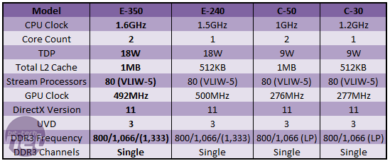
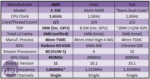
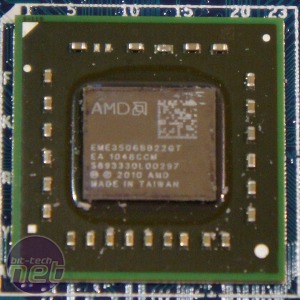
The E-350 has two 1.6GHz cores, 1MB L2 cache between them and an integrated 492MHz DirectX 11 capable Radeon graphics core. This Radeon HD 6310, as AMD brands it, is essentially a HD Radeon 5450 with its 80 VLIW-5stream processors and single channel of DDR3 memory. It is, however, a significant upgrade from the integrated graphics of AMD's 700- and 800-Series chipsets which their 40 VLIW-5 stream processors.
HTPC enthusiasts also get AMD's latest UVD 3 technology, with support for HDMI 1.4a that provides enough bandwidth for everything up to Blu-ray 3D. Dual digital display outputs are also finally supported by AMD IGPs, but it's down to the manufacturer if they want to use them. Thankfully, most motherboards we've seen come with HDMI, DVI and VGA, although DisplayPort is also an option.
As you'd expect, the chip supports DDR3 memory. The CPU's memory controller is officially limited to a 1,066MHz bus speed and single memory channel, although Gigabyte does include a 1,333MHz option despite this. This anaemic setup is designed to keep the ball-count down on the CPU package, and to keep the power use down (a higher frequency means a higher TDP). Basically, AMD would rather commit its power budget to CPU frequency rather than memory speed. Unfortunately, though, this limited bandwidth is also shared between the GPU and CPU; the GPU doesn't get to 'borrow' any cache from the CPU in the same way as it can in Intel's Sandy Bridge CPUs.
In addition, unlike Nvidia's ION chipset for old Atom hardware, the CPU can only offer four PCI-E 2.0 lanes. As such, it's worth remembering that the graphics slots on these mini-ITX boards only offer four PCI-E lanes.
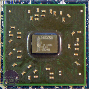
Finally we have the Hudson-M1 Fusion controller hub (FCH), which is a pretty pimped up piece of Silicon. You could look at this as AMD giving two fingers to Intel's limited adoption of SATA 6Gbps on its Sandy Bridge PCHs, and its weak offering of two SATA ports on the Atom platform. Conversely, the Hudson-M1 FCH is fitted with a full stack of six SATA 6Gbps ports. Combine this with the 18W TDP of the E-350 and you can say hello to a high-performance, low power NAS box.
AMD hasn't stated the TDP of the Hudson-M1 chip, but it's likely to be lower than the SB850's 6W TDP, as it doesn't support PCI or RAID, and it doesn't offer as many PCI-E lanes either.
We know that AMD has, for the first time, used TSMC's services to fabricate the new Brazos APUs on its 40nm high-performance process. However, unlike the 'Made in Taiwan' stamp on the APU, the FCH's stamp reads 'Made in China.' As such, the FCH is probably fabricated on a 55nm process, as with AMD's other southbridges.
We know this because there are technology export restrictions in the USA and Taiwan, which limit the fabrication technology that businesses can export into China. Intel also has a China fab, and that exclusively makes 65nm chipsets as well; no CPUs. The other reason why the FCH remains on a 55nm process is because it lowers the risk factor; AMD will just have adapted the current SB800 series to fit this platform, cutting down cost and design time.

MSI MPG Velox 100R Chassis Review
October 14 2021 | 15:04



Want to comment? Please log in.