Rear I/O
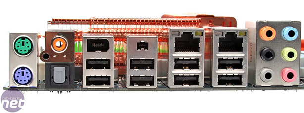
- PS2 mouse and keyboard
- Optical and RCA digital S/PDIF
- One 6-pin Firewire socket
- One 4-pin Firewire socket
- Eight USB 2.0 ports
- Two RJ45 Gigabit Ethernet sockets
- Six 3.5mm stereo audio jacks for 7.1 channel surround sound, microphone and line-in.
The only downside is that they are all right next to each other – Asus deliberately spaces its USB ports out a little, just in case someone wants to use a fat USB peripheral. However, we’d rather have the connectivity of eight and go find extension cables if need be.
Both optical and RCA digital S/PCIF are supplied, so you don’t have to choose, and there’s even an extra pair of pin-outs on board just in case you need a pass-through from an Nvidia graphics card.
We like the choice of four or six pin Firewire sockets too – it’s something that no one else does. As usual, Gigabyte is onto a winner with its rear I/O layout.
BIOS
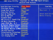
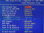
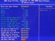
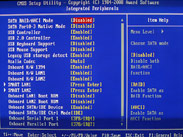
While comprehensive as you'd expect, it's not overly insane with a learning curve that's more of a gentle hill climb than a mile high rock face. There are the usual front side bus and PCI-Express frequencies available, as well as the usual "Performance Enhance" setting that we recommend turning to Extreme if you can.
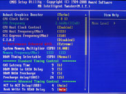
The system memory multiplier has two parts integrated into it – first, the memory multiplier itself goes up to 4x, so this allows for essentially 1:1 memory and FSB (a 1,333MHz FSB processor allows for a 1,333MHz memory bus speed). The Nvidia nForce 790i Ultra SLI had significantly more available memory control – specifically there is an unlinked mode that allows you to set the memory to (almost) anything you want. However, this kills the latency and memory bandwidth negating any clock performance increase. Intel's "limitation" means the X48 chipset can't reach super high memory speeds without processor FSB overclocking too, but at least the two buses will always remain linked with better bandwidth efficiency.
This efficiency can further be optimised by the second part listed as A-D alongside the multiplier factor. The letters represent north bridge core speeds and core latencies, where a lower MHz (and hence towards A rather than D) actually provides better performance, although in reality you have to balance both these parts as you increase the FSB and memory speed.
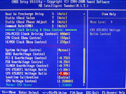
The memory timings are split into standard and advanced to make it far easier to tell what's what and to know what to adjust. Generally we start by optimising the standard timings, and then if it's still stable we dive into the advanced ones so this layout really helps keep a clear progression. Clock skews are also included now if you feel brave enough to know what's happening in the world of picoseconds without an Oscilloscope, although we'd definitely recommend using the clock drive voltage.
The voltage adjustments are quite numerous, yet clear to understand but not particularly that fine-grained in places – the GTLReference voltages particularly so, jumping in large three percent increments.
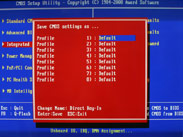
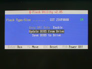
The BIOS still offers profile saving—with up to eight available—and Q-Flash, an in-BIOS BIOS flash utility (say that quickly five times in a row if you can) which is hidden behind the F8 key rather than a separate BIOS menu option.

MSI MPG Velox 100R Chassis Review
October 14 2021 | 15:04




Want to comment? Please log in.