Board Detail and Layout
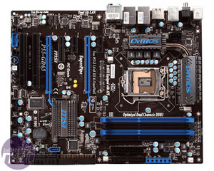
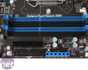
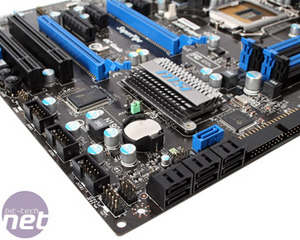
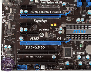
The board design is something MSI has finally nailed. While inside I long for something other than than black PCBs everywhere, I cannot deny it looks fantastic, with highlights of blue and gunmetal that really just work.The general layout is also very good, albeit like so many, not perfect. I'm sure you can clearly spot the lone blue SATA port placed inside the other six that are aligned facing towards the edge. Above this there's the IDE port still, a floppy port (again, why?), the ATX socket and MSI's V-Check Points.
This blue plastic rectangle with six square holes houses pins that offer voltage check points, so you can take a multimeter to them and get a real-time readout, without having to rely on often inaccurate software or BIOS readings. In actual fact, we found the reading to be within 0.04V of what CPU-Z stated, although a multimeter would offer a much faster and more accurate vDroop when the CPU and memory loaded. The pins offer all the important readouts: VTT, DDR, CPU and PCH voltage.
All the other pin-outs and connectors are easy to get to, placed around the edges of the board, although using the onboard base clock buttons inside a case might be a little tricky, but these are designed for benchtop testers anyway.
Quite absurdly, despite including the new OC Genie and base clock buttons in addition to the power button, MSI forgot to include the reset and clear CMOS buttons: two of the most useful. Instead we have to rely on a jumper for the clear CMOS. I can't help but feel in some instances MSI's design team got carried away with dropping on new things and forgot to use design notes from 2008, instead of 2003.
On the 2009 end of things, MSI's latest "OC Genie" is, in many ways, equivalent to Asus' RoG chips that aid overclocking. MSI told us its job is a hardware solution to help with normal overclocking, but mostly it's to do with the OC Genie button at the bottom of the board. With a single press, it automatically runs the system through a series of tests to overvolt and overclock the CPU and memory.
The whole process takes only a few seconds and is quicker than Asus' equivalent BIOS switch that does much the same thing, and unlike "auto overclocking" of the past, we found this actually works a little better giving us an overclock of 3.3GHz from a 2.66GHz Core i5-750. Not bad, but considering we can hit over 4GHz with this chip and the average enthusiast should be wanting to hit at least 3.6 to 3.7GHz, we could wish for a little more.
Both x16 PCI-Express 2.0 slots for graphics are obviously marked in blue, and match the usual single x16 or dual x8s other boards feature. The three spaces between them offers plenty of breathing room for hot cards, or super sized coolers, and the two PCI, two x1 PCI-Exress and single, open ended x4 slot allow for plenty of upgrade potential too.
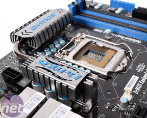
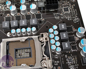
The southbridge heatsink is smaller than Asus' but it doesn't matter much because the surface area is greater, and the fins are free to vent, not to mention the fact it's also placed between the graphics card slots for slightly better ventilation. Around the CPU area the heatsinks are more meaty and have a thicker 8mm "SuperPipe" (as MSI brands) to shift heat between them. The DrMOS MOSFETs are also included for the CPU as well, in a 6+1 setup for CPU and Uncore respectively.
Each DrMOS contains up and down MOSFETs and driver IC in a single package - each can typically handle the power requirements as well as any 12 to 16-phase design from Asus or Gigabyte. Only EVGA uses the same as MSI (although do not brand it DrMOS) and typically uses more because of the greater lean towards the extreme overclocking end of the market.

MSI MPG Velox 100R Chassis Review
October 14 2021 | 15:04




Want to comment? Please log in.