Rear I/O panel:
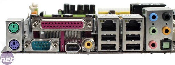
The rear I/O is pretty packed out with old and new. It’s a standard MSI layout that still features both Parallel and Serial ports, as well as the more usual PS/2. Then next to this is a 6-pin Firewire port and Coaxial S/PDIF, then four USB 2.0 sockets in a 2x2 arrangement topped off with the two RJ45 Gigabit Ethernet sockets - the left one is powered by the PCI-Express controller. Finally there are the five 3.5mm audio jacks and optical S/PDIF out.You have all bases covered here, for those who want to upgrade but are still holding on to an ageing Parallel LCD/VFD. Or maybe you work in a scientific environment that has equipment using the old RS232 standard, but fancy some gaming on the side while tests are running at home? The latter is probably unlikely though and it would have been more beneficial to include another two USB 2.0 ports instead of one or all of the legacy ports. Having said that, the K9A's rear I/O panel is a bit of everything that covers most bases and we can’t argue with that.
BIOS:
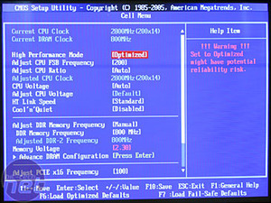
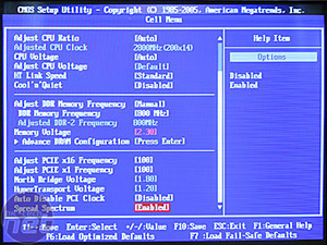
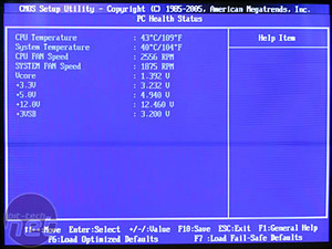
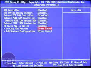
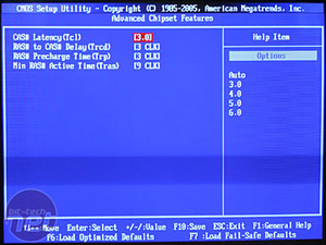
Frequency Adjustments:
CPU FSB Frequency (200-400MHz in 1MHz increments), CPU Ratio, Hyper Transport Link Speed ("Standard" or "For Overclocking"), DDR Frequency (400-800MHz), PCI Express x16 (100-200MHz in 1MHz increments) and x1 Frequencies (100-107MHz in 1MHz increments).MSI includes plenty of space for overclocking, although we aren't quite sure what "For Overclocking" amounts to in the Hyper Transport Link Speed option. We assume it clocks down the multiplier to allow for less LDT stress when increasing the CPU bus. Whilst a PCI-Express x16 frequency adjustment of up to 200MHz is fantastic, offering just 7MHz on the PCI-Express x1 bus is just worthless to overclocking. It may offer some extra stability by running the bus out of sync to the x16 bus, so you don't need spectrum spread as the data is less likely to interact across buses.
Voltage Adjustments:
Northbridge Voltage (1.8-2.15V in 0.05V increments), Hyper Transport Voltage (1.2-1.5V in 0.05V increments), DDR2 Memory Voltage (1.8-2.10V in 0.05V increments and 2.10-2.30V in 0.1V increments), CPU Voltage (1.200-1.450V in 0.025V increments), Additional CPU Voltage (3.3% to 23.3% in 3.3% increments).Voltage increments are pretty good without being so extreme that you will kill everything if you're inexperienced in the realms of overclocking. However, the CPU voltage can potentially be increased to a dangerous 1.75V when combining CPU additional voltage and increasing the standard voltage all the way. It has all the necessary basic adjustments for overclocking.
Memory Timings:
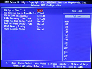
CAS Latency (Tcl), RAS to CAS Latency (Trcd), RAS Precharge (Trp), RAS Active Time (tRAS), Row Cycle Time (tRC), Row Refresh Time (tRFC), Row to Row Delay (tRRD), Write Recovery Time (tWR), Write to Read Delay (tWTR), Read to Write Delay (tRWT), Command Rate, Async Latency Value.There are plenty of useful memory timings, and if you're just concerned with the "essential" four (CAS Latency (Tcl), RAS to CAS Latency (Trcd), RAS Precharge (Trp), RAS Active Time (tRAS)) these are in a separate location to the Cell Menu under Advanced Chipset Features. To those who are more experienced with BIOS optimisation, this will be annoying because it means you have to navigate out and in between sub-menus rather than having everything on the same page. There's enough to make it enjoyably tweakable and keep someone busy, but not so many that it dwarfs and confuses you.
Other Inclusions:
Enable/Disable each LAN controller independently, Firewire controller and HD Audio.The ability to enable or disable all the extra on-board components so they don't use excessive resources is also a bonus. It also means because the rear Ethernet ports are indistinguishable, that you can select the more efficient PCI-Express one for preference. Overall MSI delivers with a reasonably comprehensive but straight forward BIOS.

MSI MPG Velox 100R Chassis Review
October 14 2021 | 15:04


Want to comment? Please log in.