PCB, Cooling and Power
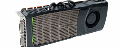
The card itself looks unlike any other graphics card we’ve seen before, with the 10.5in PCB utterly dominated by the huge quad heat-pipe cooler sat atop the GF100 GPU which pokes through the external plastic shroud - it gives the GTX 480 a unique industrial look.The card comprises four separate pieces screwed together. If you're taking the card apart, first comes the black plastic shroud, held in place by six plastic clips and easily removed to reveal the meaty cooling solution beneath. The heat-sink assembly is attached separately to the rest of the cooler and is held in place by four screws positioned at either corner of the GPU.
The heatsink itself is composed of five nickel plated copper heat-pipes, machined flat as to be in direct contact with the GPU, in a similar way to many modern CPU coolers like the Titan Fenrir. The heatpipes then run out through the heatsink’s cooling fins which are set horizontally, allowing air to pass from the cooling fan to the back of the card.
Uniquely, the heatsink’s top plate actually extends through the plastic top shroud, exposing the large metal surface. Presumably this is to optimise cooling although we’ve seen that some board partners plan to place branding stickers on this surface so presumably it’s not a critical part of the card’s cooling.
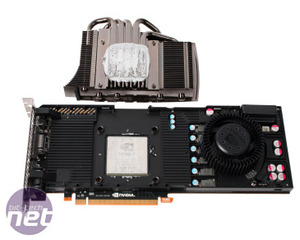

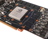
Click to enlarge - The GPU heatsink is attached separately to the rest of the cooler, as with the GTX 295
The third segment is a large aluminium plate which sits atop the card’s memory and power circuitry to provide additional cooling, and it's held in place by eleven separate screws. This plate is where the card’s 65mm paddle fan is fitted, driving air the 7in from the back of the card through the heatsink and out the rear I/O plate. Sadly during the removal of this plate we managed to throw a screw's threading, and during an attempt to dremel the screw free managed to drill a neat hole into the PCB, breaking our card. Luckily we'd already done all our testing for this article though!
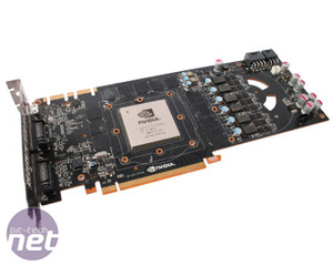
Having removed the three separate layers of shroud, heatsink and aluminium plate we finally come to the PCB, measuring up at 10.5in long (a little shorter than the HD 5870). While the huge GF100 GPU sits at the card’s heart around it lie twelve Samsung K4G10325FE 128MB GDDR5 modules, with three to the left of GPU, five above and four to the right. Beneath where the paddle fan is fitted there are two small cut outs to allow air intake from the back of the board as well as the front. We’ve previously seen this technique from Nvidia when it launched the original dual PCB GTX 295.
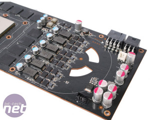
The potential 250W of board power is provided care of one eight pin and one six pin PCI-E power connector angled upwards on the card. Power is then delivered by a suitably high end power delivery system, composed of six phases for the core and a single heavier duty phase for the memory. Nvidia has chosen to not use digital power switching, unlike ATI, but the six chokes will generate less heat due to the components being spread over a wider area.

MSI MPG Velox 100R Chassis Review
October 14 2021 | 15:04




Want to comment? Please log in.