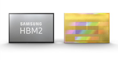
Samsung has taken the opportunity of Nvidia's GPU Technology Conference to announce Flashbolt, a High Bandwidth Memory 2 implementation it claims is a third again faster than the company's previous offering.
Designed, Samsung claims, for next-generation supercomputers, graphics systems, and artificial intelligence (AI) systems, Flashbolt is claimed to be the first HBM2E implementation to offer 3.2 gigabits per second (Gb/s) throughput - 33 percent faster than Samsung's previous-generation HBM2. Each Flashbolt die offers a 16Gb data density, double that of its predecessor, giving a single Flashbolt HMB2E package a claimed 16GB overall capacity and 410 gigabytes per second (GB/s) throughput.
'Flashbolt's industry-leading performance will enable enhanced solutions for next-generation data centres, artificial intelligence, machine learning, and graphics applications,' claimed Jinman Han, senior vice president of the Memory Product Planning and Application Engineering Team at Samsung Electronics, of the new design. 'We will continue to expand our premium DRAM offering, and improve our high-performance, high capacity, and low power memory segment to meet market demand.'
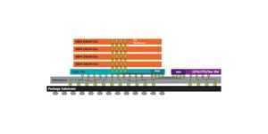
Flashbolt comes just over a year after Samsung announced Aquabolt, itself replacing the earlier Flarebolt, which offered 8GB capacity and 307GB/s throughput per package. That design was based on a 3D stack of eight 8Gb dies connected using over 5,000 through-silicon vias (TSVs) per die - a technique which is almost certainly duplicated in its successor, Flasbolt.
Full details of the Flashbolt technology, including design wins, have not yet been provided by the company, but with it being positioned initially at the high-profit low-volume end of the market expect it to be a while before Flashbolt appears in consumer products.

MSI MPG Velox 100R Chassis Review
October 14 2021 | 15:04


Want to comment? Please log in.