The JEDEC Solid State Technology Association, formerly known as the Joint Electron Devices Engineering Council, has announced an update to the High Bandwidth Memory (HBM) standard, pushing higher densities, increased bandwidth, and support for through-silicon via (TSV) stacks up to 12 layers high.
Designed, as the name implies, for cases where bandwidth is king, High Bandwidth Memory (HBM) has become the go-to memory type for high-performance compute products - including graphics cards, where it has supplanted Graphics Double Data Rate (GDDR) at the highest end. Officially standardised by the JEDEC Solid State Technology Association as JESD235 High Bandwidth Memory (HBM) DRAM, HBM now has a boost in the form of a standard update promising improved densities and performance.
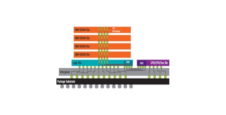
Dubbed JESD235B, the new variant adds support for 12-layer through-silicon via (TSV) stacked packages - a form of three-dimensional chip-building where multiple layers of silicon can be formed one on top of the other and connected using tunnels, known as vias, through the other layers - which extends the maximum capacity of a single HBM device to 24GB based on current 16Gb-per-layer densities. The new standard also incorporates Wide Input/Output (Wide I/O), moving to a 1,024-bit device interface split into eight independent channels per stack and delivering throughput of up to 307GB/s at 2.4Gb/s per pin.
The release of a new standard, however, does not mean hardware is around the corner: JEDEC has not indicated when its member companies are likely to adopt the JESD235B revision.


MSI MPG Velox 100R Chassis Review
October 14 2021 | 15:04

Want to comment? Please log in.