An Overview of High-Bandwidth Memory (HBM)
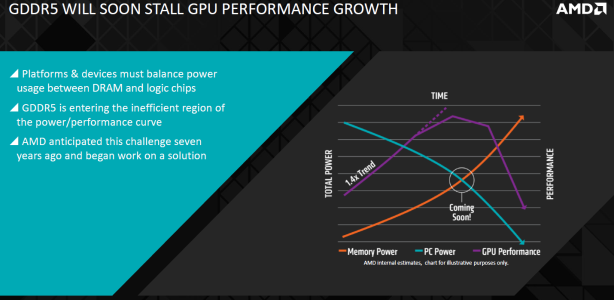
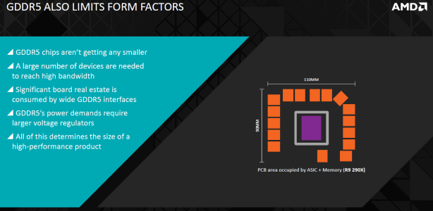
GDDR5 has long been established as the DRAM of choice for high-performance graphics, and is presently used in all current high-end and mid-range graphics cards and also in the PlayStation 4. However, as the bandwidth demands of GDDR5 continue to grow, so too does its power requirements. As graphics processing is inherently power limited, feeding the memory more power means less available watts for the GPU in any given environment, and GDDR5 is now approaching the stage where the power needed to supply the memory bandwidth modern GPUs require is so high that it's not leaving enough for the GPU itself, causing a performance flatline. This is not a new phenomenon; it is predictable, and AMD and its partners have been working on a solution for some seven years now.GDDR5 also presents a form factor limitation, as the chips aren't getting any smaller. While the very latest chips are dense and capable of fast data rates (Samsung's 8Gbit ones are certified for 8Gb/sec), their 32-bit interface means you still need a large number of devices to reach a high total bandwidth. This eats up PCB space, as do the large VRMs required to handle the power demands.
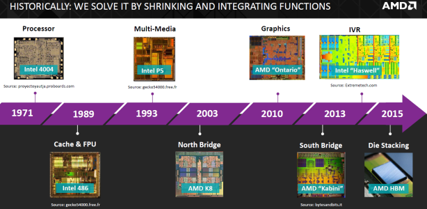
These problems are typically solved by shrinking and integrating components onto the main processor die. However, this is not really a viable option for DRAM; it is neither cost nor size-effective. Simply put, processors and DRAM are disparate, meaning they are built in very different ways and have different requirements. The logic wafers required for processors are very expensive, and the build process is not specialised for DRAM use either. This would likely force the use of a larger cell size for the DRAM, meaning you'd need to use even more of the very expensive wafer to integrate it and would end up with a very big, very costly chip.
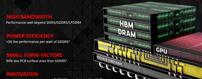
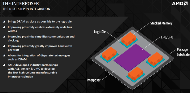
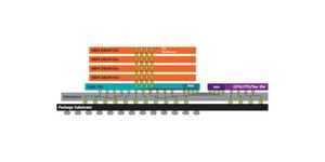
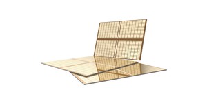
With scaling upwards off-chip and integrating on-chip both being impractical and too costly in more ways than one, a middle ground is needed. The solution is a silicon interposer, which is literally a middle ground between the main logic processor and the DRAM dies. The interposer sits atop the package substrate, so the processor and DRAM will now come in a single package – it's a much more integrated solution than before, but the two components are not on the exact same die. Nevertheless, there is a direct, short connection between the two through the interposer, and this much greater proximity allows data to be transferred across an extremely wide memory interface. This also means much lower clock speeds can be used (since so much can be transferred in a single clock cycle), which means the power per bit is down and the bandwidth per watt is up.
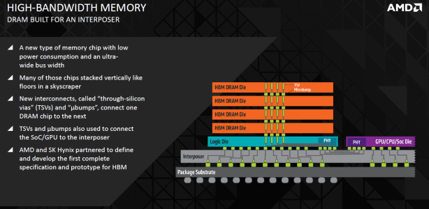
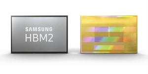
With its much wider memory bus, the new design requires a new type of memory, known simply as high-bandwidth memory, or HBM, and a key feature of HBM is that it's designed in 3D – individual dies can be stacked atop one another, and the entire stack rests on the logic die beneath, through which the connection to the processor is made. Achieving this is obviously complex, but it relies on two key things. Firstly, the DRAM wafer needs to be extremely thin for stacking to work effectively. AMD gave us a figure of 100 microns, which is literally paper-thin, and indeed the wafer will actually flop like a piece of paper at this thickness. Then there is the question of connecting the dies, for which a new interconnect known as a through-silicon-via, or TSV, is used. A TSV is essentially a hole poked vertically through the thinned silicon wafer and filled with copper. Each die has multiple TSVs, and when stacked, they are joined using high-density solder microbumps – this process also connects the processor to the interposer. While it is undoubtedly a complex assembly process, it results in extremely short interconnects between dies, which has benefits for small form factors, latency and power consumption.
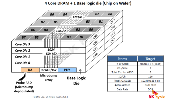
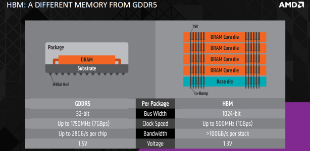
In its present form, a single stack of four HBM dies has a total bus size of 1,024 bits through eight, independent 128-bit channels (two per die). The 1GHz effective clock speed makes for a total bandwidth of 128GB/sec per stack. Importantly, the required voltage is also lowered – AMD says it's 1.3V, although all other information we've seen points to 1.2V. Either way, it's lower than GDDR5, which typically runs at 1.5V but also has a 1.35V specification.

MSI MPG Velox 100R Chassis Review
October 14 2021 | 15:04



Want to comment? Please log in.