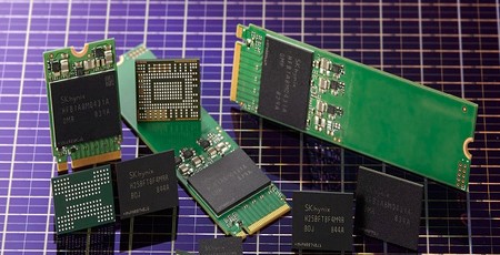
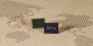
Memory maker SK Hynix has announced its first NAND flash design based on 96-layer triple-level cell (TLC) charge trap flash (CTF) with periphery under cell (PUC) technology, offering 512Gb (64GB) per chip - which, for some reason, it has opted to claim is 'four-dimensional'.
Announced this week, SK Hynix' development is a veritable alphabet soup of related technologies all combining to reduce the size and thus increase the density of NAND flash components. Using a now standard multi-layer 3D stacking design hitting an impressive 96 layers deep, the company's creation combines four key technologies: triple-level cell (TLC), which increases the amount of data each NAND flash cell can store; charge trap flash (CTF), which dates back to early electrically erasable programmable read-only memory (EEPROM) designs and in modern SSDs replaces floating gates to reduce chip size and manufacturing costs while boosting reliability; and periphery under cell (PUC), which places IO components underneath rather than at the edge of cells in order to further reduce size - a first when combined with CTF, SK Hynix claims, with the technology previously having been restricted to 3D floating gate designs.
Combined, the technologies boost the SSD chips considerably: When compared to the company's previous 72-layer 512Gb NAND chips, SK Hynix claims, the new design drops chip size by 30 percent, improves 'bit productivity per wafer' - the amount of usable storage the company can produce from a single silicon wafer, a metric which combines density and yield - by 49 percent, and when installed in a finished product boosts write speeds by 30 percent and read speeds by 25 percent.
'This 96-Layer CTF-based 4D NAND, with the industry's top cost competitiveness and performance, will become a milestone in the company's NAND flash business, as a platform in developing future products,' claims SK Hynix vice president and head of NAND marketing J. T. Kim, apparently fully in favour of his company's decision to claim the design breaks into the fourth dimension. 'The company plans to start the early stage mass production of it within this year and further expand the production in M15 to actively respond to a variety of clients.'
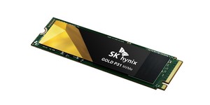
SK Hynix has confirmed it plans to launch consumer-oriented 1TB SSDs based on the parts, coupled with in-house controllers and firmware, before the end of the year, with enterprise variants due in the second half of 2019. The company has also updated its roadmap with the promise of Universal Flash Storage (UFS) 3.0 parts for mobile devices in the first half of 2019, along with the promise of 96-layer NAND flash components hitting 1Tb (128GB) and based on triple-level and quad-level cell (TLC and QLC) technologies before the end of 2019.


MSI MPG Velox 100R Chassis Review
October 14 2021 | 15:04

Want to comment? Please log in.