AMD 790GX IGP
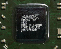
The 790GX, or HD 3300, is a mere evolution of the 780G, or HD 3200 - both include an RV610 core which features 40 unified stream processors that are DirectX10, not 10.1 capable. The difference being that the GPU clock has been increased from 500MHz on the 780G to 700MHz on the 790GX.In many ATI chipsets in bygone years have we seen the availability of using a local frame buffer - basically a single memory chip the IGP could access directly to speed things up a bit. However no one ever used it - it simply added cost making the board uncompetitive for very little benefit.
Back when the 780G launched we again saw the option of this local frame buffer and we specifically asked AMD, will people use it this time? A very astute AMD replied, "yes, yes! We've got many partners who have committed to using it!" Did words translate to products? Unsurprisingly, no.
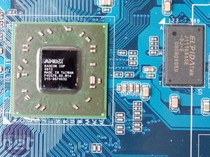
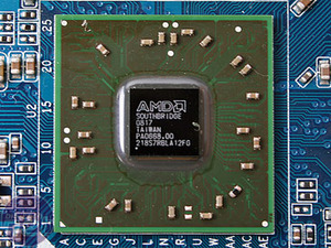
From left to right - the 790GX northbridge, the Elpida 128MB 1,333MHz DDR3 local frame buffer and the SB750. Click to enlarge.
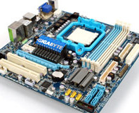
The problem was, integrated graphics was seen as something value, not performance: the focus is on cost not features. Things look a little different this time around though as AMD has positioned the 790GX as a performance part above the 780G. With increased memory density and now the greater availability of affordable DDR3, board makers like Gigabyte have jumped on this and included 128MB of 1,333MHz DDR3. At low resolutions this should, for the first time, make quite a bit of difference.
The HD 3300 can still address an extra 512MB of system memory, but at the time of publication we still waiting for a response from AMD with regards to whether the HD 3300 can use the local frame buffer exclusively if the BIOS is set to use the exact amount supplied on board (128MB on the Gigabyte board for example), so it doesn't impede on your main memory performance. In further testing we've found that the IGP can lower performance of the whole system, so possibly avoiding this should be beneficial to some degree.
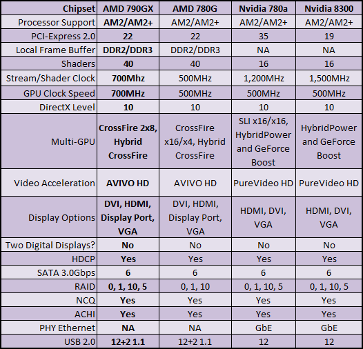
As we can see from the table, the 790GX supports a balanced PCI-Express 2.0 x8 by x8 CrossFire, unlike the 780G. In contrast, Nvidia uses its NF200 chip on the 780a to convert one PCI-Express 2.0 x16 lane into two x16 lanes. Despite being able to split the PCI-Express lanes on the 790GX, the only other difference is that the IGP now runs at 700MHz rather than 500MHz, however many were able to overclock the 780G to 800MHz or 900MHz (given decent cooling) making this a small bump at best. AMD still uses a single clock domain for its 40 Stream processors, unlike Nvidia which has just 16 clocked at 1.2GHz to 1.5GHz.
Dual displays are still supported but there is still no support for a second digital output - you have to choose between HDMI, DVI and even DisplayPort, all of which offer HDCP encryption. UVD is also still the same, with its internal S/PDIF passthrough for 5.1 audio and complete processing offloading of MPEG2, AVC (H.264), and VC-1 content.
Nvidia matches this offload capability with its PureVideo HD and even includes Picture-in-Picture function with the latest Cyberlink PowerDVD 8 Ultra patch. While Nvidia's method of audio processing is crude - requiring a loopback cable from the soundcard because its chipsets do not have an internal audio processor, it does support the HDMI 1.3a specification in as much as it allows LPCM 7.1 channel HD audio bitstream over HDMI, although this does not include Dolby TrueHD and DTS-HD Master Audio. AMD currently does not offer this with its integrated graphics UVD.
SB750 - Fixed & Ready To Go
Now its clock generator is fixed and AMD has bolted on RAID 5 into the mix, AMD now (finally) has a southbridge to match the competition. AMD's USB performance has also been notoriously weak and the company has maintained that this has been improved through SB700 and now SB750. We put this claim to the test very soon.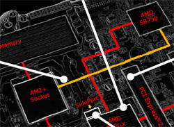 The most interesting feature of the southbridge is its new Advanced Clock Calibration feature. Unfortunately we can only allude as to what this does technically because AMD hasn't yet told us specifics, although from the name we can obviously tell it's a new embedded controller that keeps the clock generators in sync as the clock speeds are changed out of spec when overclocking.
 Gigabyte told us that it was specifically designed for Phenom X4 Black Edition CPUs, allowing either a greater overclock or a lower voltage for the same overclock. The fact it mentions Black Editions specifically means that it works best when you're only increasing the multiplier affecting the CPU frequency only and not increasing the HyperTransport affecting the system as a whole.
The diagrams link the southbridge to CPU and we can only assume the pre-AM2+ SB600 southbridge was designed without any calibration functions, and with SB700's clockgen failure, we've had to wait until now to get the full CPU-northbridge-southbridge all up to date and designed to work together.
Finally, what is now completely off the radar is the HyperFlash support, an AMD equivalent to Intel ReadyBoost NAND Flash, AMD had claimed to be putting on the 700-series chipsets when we discussed Puma and Griffin a year ago.

MSI MPG Velox 100R Chassis Review
October 14 2021 | 15:04




Want to comment? Please log in.