What’s in a Phenom anyway?
We covered the general parts to AMD’s quad-core architecture back in May, so we’ll refresh your memory a little while giving you a bit more detailed information on the subject.Just to reiterate: all Phenom processors work in current AMD AM2 boards, but they will likely require a BIOS update. That is on the proviso that your motherboard is still actively supported by its manufacturer.
The reason we say this is because there has only been one new chipset for AMD’s CPUs—the AMD 690G—in the last year, and as a result there might be some Taiwanese companies that have dropped BIOS development for older products.
More importantly however, all current Athlon 64 X2 AM2 CPUs will fit in the newest AMD 700-series chipset motherboards with AM2+ sockets, however this doesn't automatically mean your AM2 CPU will be able to take advantage of AM2+ features.
Using a Phenom in the latest AM2+ board is obviously the most ideal option, not just because it’s simply newer but because it offers separate power planes between the four cores and the ‘north bridge’ (in other words, the memory controller and L3 cache). This allows them to independently clock themselves down to reduce power consumption when they’re sitting in an idle state.
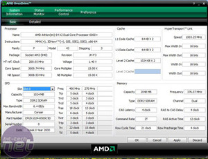
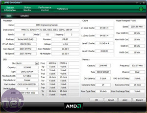
While AM2 CPUs have an identical clock between memory controller and CPU, the potential with Phenom was to run the memory controller at a higher frequency than the CPU cores, allowing the whole system to be more efficient. However, the opposite has turned true – the Phenom memory controller is currently stuck at 2GHz, regardless of what we ran our core speeds at.


Comparing the Athlon 64 X2 6000+ to the Phenom in AMD's Overdrive utility we can see the differences
The Phenom CPUs themselves each have three cache levels – the last time we saw this was with Intel’s Extreme Edition “Galatin” cored Pentium 4 CPUs that were basically single core Xeons shoehorned into a socket 478 package. While the “server core on the desktop“ isn’t true with Phenom (as AMD calls its server chip “Barcelona” while its desktop chip is called “Agena”), the L3 cache now serves four cores not just one.
Fundamentally, the basic L1 and L2 cache architecture hasn't changed from the K8 core: each of the Phenom cores has 128kB L1 cache split into two 64kB pools to separate instructions and data, along with a 512kB L2 data cache. Comparatively, Intel’s larger 4MB or 6MB L2 cache is shared between pairs of cores, so in a quad-core chip there is 8MB or 12MB to go round. Being L2 it’s not only far faster but lower latency than the L3 cache on the Phenoms – however, this large cache is also used as compensation for the lack of an integrated memory controller on Intel CPUs.
The execution core is essentially the same as the one used in the K8 architecture, but it’s been widened in parts like SSE handling, which has had a top to bottom 128-bit upgrade so that it can now handle SSE instructions in a single clock cycle. Phenoms have also received an incremental upgrade of HyperTransport from version 2.0 to 3.0, which represents a clock upgrade from 1.0GHz to 2.0GHz, although the core HyperTransport bus speed is still 200MHz.
The FX range, which was supposed to be making a return back to the LGA1207 Opteron server socket, has suddenly disappeared and when we quizzed AMD about this, we received a reply saying that there is nothing to still officially disclose. Whether this is a sign of canning the FX range, like AMD has already partly done with the 4x4 enthusiast system recently, we're uncertain.
Finally there's also the improved Virtualisation, codenamed “Trinity” which is Nested Paging in a virtualised environment – this is an improved method of memory switching compared to the older Shadow Paging technique. In addition there is also a Tagged Execution Buffer and Translation Look-aside Buffer. You can read the details of both of these in our original Phenom architecture piece.

MSI MPG Velox 100R Chassis Review
October 14 2021 | 15:04


Want to comment? Please log in.