
AMD's Upcoming hardware: The stress of 32nm High-K Metal Gate + new design
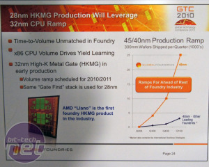
We know from AMD's own admissions, although detailed further by Global Foundries in its presentations; AMD's 'Llano' Fuzion APU will debut next year on its 32nm High-k Metal Gate 'Super High Performance' process. AMD's own slides are slightly confusing because it claims both SOI (silicon on insulator) and High-k MG technologies are in use.AMD needs all the help it can get though, because Llano and its high performance Fuzion brothers will be a monumental effort. For starters it's still AMD's first entirely new core for five years, then throw on graphics into that mix and then chuck in a smaller and newer High-k MG process technology. Now, finally, add to the fact that Global Foundries admits that Llano is 'driving yield learning' for its 32nm process (!) and AMD's most important product in its history is facing truly insurmountable odds.
It's not even being helped much by experience from its Ontario and Zacate parts either, because TSMC is manufacturing those. Global Foundries already offers a 40nm 'low power' option, but that appears not cover the diverse needs of x86. In contrast Ontario and Zacate should be easy to make for AMD and TSMC as it combines the familiar K10.5 x86 core parts, with the fact that TSMC already makes the Radeon GPU portion. All this goes into a relatively small (albeit packed) die and lower ~400M transistor count (in contrast even the Radeon 5600 series has 50 per cent more transistors).
Next stop, 28nm!
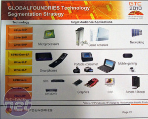
Whereas TSMC cancelled its 32nm node entirely concentrating on High-k MG launching only on 28nm; apparently sometime around now, although we think TSMC's roadmaps are optimistic at best - Global Foundries on the other hand, is firing ahead with High-k metal gate at both 32nm and 28nm.The 32nm node is its 'High Performance' technology, which is already well into development, with real products (AMD Llano) arriving somewhere into the first half of next year.
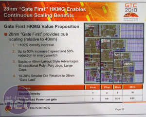
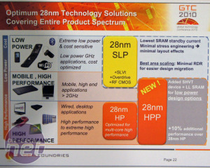
28nm uses the same production technology as 32nm, but Global Foundries design is for lower power, lower leakage devices only: it's not suitable for CPUs. Compared to 40nm, 28nm cuts the same die size in half (and future 20nm goes half again), while promoting a 50 per cent increase in switching speed and energy reduction per switch.
Both Global Foundries and TSMC are hitting the 28nm stride about the same time, but the difference between both companies is that where Global Foundries is putting its 'High Performance' stamp on 32nm, TSMC is pushing the same thing at 28nm having learnt from its previous expertise in high performance half-nodes at (110nm, 80nm,) 55nm and 40nm.
These competing roadmaps are not directly comparable however, and the specialisation of part type and techniques of manufacturing will see who gets the customer. For 28nm at least, both AMD and Nvidia should be sticking with TSMC. The next question being: will it hurt AMD for sticking to 40nm in its upcoming Radeon HD 6000 series?
Beyond that, direct competition could potentially offer competitive pricing between the two companies, which means cheaper chips for us.

MSI MPG Velox 100R Chassis Review
October 14 2021 | 15:04




Want to comment? Please log in.