
22/20nm and beyond
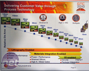
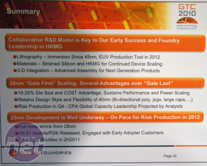
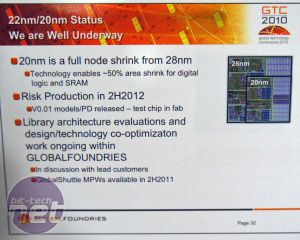
Global Foundries explained that its collaboration with other giant chip fabs we listed previously, would enable it to have the resources to reach future process nodes such as 22/20nm. Immersion extreme UV and High-K metal gate will continue to play at part in that, but it would be an understatement to say that there are ever increasing technical challenges, and not only in silicon manufacture, but in associated packaging technology too; with things like 3D chip stacking to increase performance density. This will be particularly important in the smartphone and tablet market where physical space is a premium.Global Foundries limited comments on its 22/20nm node to just a single slide, claiming it was 'well underway' for sometime in the second half of 2012. We understand the focus now is on telling customers about its 32/28nm nodes in the immediate future, however we certainly weren't convinced developments beyond that are in anyway solid.
Partnership with ARM
Global Foundries was keen to push its partnership with ARM, presumably to break from the Global Foundries = AMD mould. ARM's dual-core A9 reference hardware has already been taped out on 28nm 'High Performance' node, which the company claims gives a 500MHz frequency bump for 15 per cent less voltage, but there was no specifics with regards to products from ARM design partners such as Texas Instruments, Samsung and Marvell at this time.Along with fine grained power gating, this more delicate power-performance balance is where Global Foundries could really set itself apart though, as it cannot compete with in x86 versus Intel, but it can challenge it in the mobile space where ARM is on a charge.
Where are the 450mm silicon wafers?
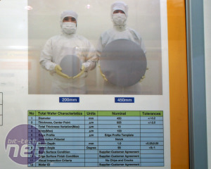
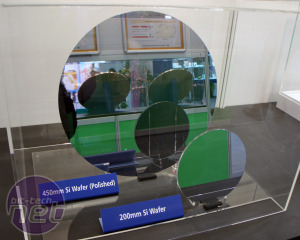
Right now, 450mm wafers appear to be MIA. The current 'large standard' is 300mm (about 12 inches) but 200mm (8 inch) wafers are still used by Global Foundries for some specific IC production,although it still accounts for massive 176,000 wafers a month from the Singapore fabs. The industry movement to a much larger 450mm (18 inch) wafers was expected between 2012-2014 but various reports state that being put back a year or two by other companies, despite the fact we've already witnessed a supporting industry ready(ing) in recent trade shows.450mm is needed to reduce the costs of production. As each wafer has more or less a set production cost, going bigger simply invokes economies of scale. The problem lies in the initial investment in hardware to handle those extra six inches - and with each smaller generation node getting more difficult to produce, companies are less willing to take risks on multiple new manufacturing techniques.
We contacted Global Foundries to ask about a 450mm commitment and were told the company had adopted a 'wait and see approach' on the supporting industry it claims is not yet ready, and it was looking at long term plans of 7-10 years from now! Wow!
Given then Global Foundries is so keen to get its New York Fab 8 ramped up to add to its most advanced process capacity; why hasn't it used the opportunity to trial 450mm equipment, which would achieve the capacity ramp that much better? Especially if they are buying new equipment to fill that new fab.
While Global Foundries can throw billions to increase its wafer capacity, in light of what the rest of the industry is doing, we're still unsold on it's technological decisions and its first 'non-AMD' 32/28nm process move next year will certainly be a defining start - either good, or bad.

MSI MPG Velox 100R Chassis Review
October 14 2021 | 15:04




Want to comment? Please log in.