Hybrid Memory Cube specification gets finalised
April 3, 2013 | 10:38
Companies: #hybrid-memory-cube-consortium

The Hybrid Memory Cube Consortium, the industry group responsible for creating three-dimensional high-speed memory based on stacking layers of DRAM connected using through-silicon vias (TSV,) has officially announced the finalisation of the HMC Specification - opening the floodgates for manufacturers to start implementing the technology.
The Hybrid Memory Cube technology is the work of a group of DRAM industry giants including Samsung, Hynix and Micron - the latter of which picked up an award for the technology in January last year, when its prototype modules hit an impressive throughput of around 128GB/s - and recently welcomed Microsoft into its ranks. So far, though, while prototype products have been demonstrating impressive potential, offering data throughput some ten times higher than traditional DDR3 memory, purchasable products have been thin on the ground.
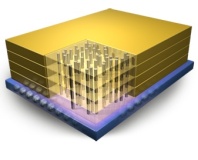
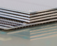
The system works by utilising through-silicon vias (TSV) which allow layers of silicon to be built one on top of another and interconnected using conductive channels - 'vias' - that pass through each layer of silicon to the next. The result is a dense design that packs the capacity of multiple memory modules into the footprint of a single module, while offering extremely short signal paths between layers. In testing, Micron was able to show a boost in peak data throughput of ten times that offered by traditional two-dimensional planar memory construction, while simultaneously dropping the power draw by 70 per cent and the size of the finished module to one-tenth that of current products.
Doing that in the lab is one thing, but actually producing something people can pick up requires the various companies involved - which, in addition to those named above, includes the like of Altera, ARM, HP, IBM, Open-Silicon and Xilinx - to sit down and agree to a finalised specification that manufacturers can use to guarantee interoperability. Back in May last year, the Hybrid Memory Cube Consortium had promised that the finalised specification would be available by the end of 2012 - but it sadly missed its self-imposed deadline when the year ended with no sign of the specification.
Better late than never, the group has now released version 1.0 of the specification (PDF warning) offering manufacturers the chance to start gearing up to produce commercialised implementations of the hardware without fear of taking a wrong turn that will result in an incompatible design.
'The consensus we have among major memory companies and many others in the industry will contribute significantly to the launch of this promising technology,' claimed Jim Elliott, vice president of memory planning and marketing at Samsung's semiconductor arm. 'As a result of the work of the HMCC, IT system designers and manufacturers will be able to get new green memory solutions that outperform other memory options offered today.'
'This milestone marks the tearing down of the memory wall,' added Robert Feurle, vice president of DRAM marketing at Micron. 'The industry agreement is going to help drive the fastest possible adoption of HMC technology, resulting in what we believe will be radical improvements to computing systems and, ultimately, consumer applications.'
'HMC is a very special offering currently on the radar,' concluded JH Oh, SK Hynix's vice president of DRAM product planning. 'HMC brings a new level of capability to memory that provides exponential performance and efficiency gains that will redefine the future of memory.'
A standard does not a product make, however, and while plenty of vice presidential types from HMCC's member companies were only to happy to provide soundbytes as to the breakthrough that has been made and the potential for HMC to change the face of computing forever, none were willing to suggest when the first modules will actually appear in consumer products. The group is already looking to revision 2.0 of the specification, however, promising to double data rates by the time the second specification is formalised in early 2014.

MSI MPG Velox 100R Chassis Review
October 14 2021 | 15:04


Want to comment? Please log in.