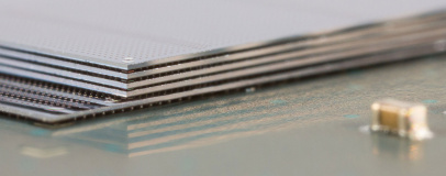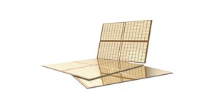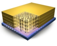
Micron has officially started shipping its first Hybrid Memory Cube (HMC) devices, using through-silicon vias (TSVs) to stack four 4Gb DRAM dies into a single 2GB cube.
Micron's early work on three-dimensional memory resulted in an award back in January, which caused enough of a stir for Microsoft to enter the HMC Consortium and put its own not-inconsiderable weight behind the standard. The specification itself was finalised back in April, with Micron promising it would begin production as soon as possible.
The company has now delivered on its promise, producing the first commercial HMC devices and offering engineering samples to its customers immediately, ahead of mass production.
The engineering sample devices offer 2GB of storage with a claimed 160GB/s transfer rate in a compact footprint with a 70 per cent reduced power draw per bit compared to traditional planar memory layouts. The HMC works by allowing chips underneath the stack to communicate with those on top, and vice-versa, using electrical conduits known as vias which pass through the silicon of the chip itself - hence 'through-silicon vias.'
'System designers are looking for new memory system designs to support increased demand for bandwidth, density, and power efficiency,' claimed Micron's Brian Shirley, vice president of the DRAM Solutions group, at the announcement. 'HMC represents the new standard in memory performance; it's the breakthrough our customers have been waiting for.'
In addition to the 2GB engineering samples available now, Micron has promised to produce 4GB versions in early 2014 ahead of volume production of both later that year. The company is so confident of the technology's success, in fact, that it claims it will take just three to five years for the first mainstream HMC-enabled consumer products to appear on shop shelves.

MSI MPG Velox 100R Chassis Review
October 14 2021 | 15:04


Want to comment? Please log in.